The UCF Nanofabrication Shared Facility is composed of three complementary cleanrooms located in the College of Optics and Photonics (CREOL), the College of Engineering and Computer Science (CECS), and the College of Sciences. These open-access facilities are available to UCF faculty and students, external academic researchers, and industrial partners seeking advanced prototyping and R&D capabilities.
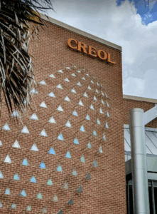
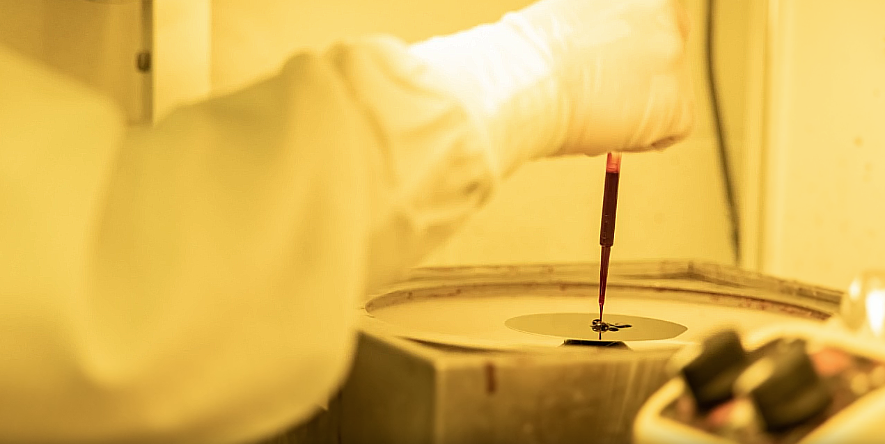
The CREOL Nanofabrication Facility (CNF) consists of 2,100 square feet of Class 100 and Class 1000 cleanrooms with standard optical lithography, deposition and etching tools, as well as a 100kV Raith 5200+ e-Beam Lithography instrument capable of 10-nm resolution. CNF is used for the fabrication of integrated photonic devices and circuits, as well as nanostructured materials and samples.

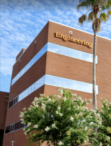
The CECS Nanofabrication Facility is a multi-user laboratory dedicated to supporting university researchers, as well as industrial and government partners. The facility offers a full suite of tools for 4-inch-diameter substrate processes, including lithography, deposition, etching, and characterization.
Highlights include atomic layer deposition (ALD), ultra-high-vacuum (UHV) PVD systems, a mask aligner with UV lithography, and a plasma-enhanced chemical vapor deposition (PECVD) system. We are especially proud of our latest addition—the Heidelberg DWL 66+ laser lithography tool, which offers a minimum resolution of 600 nm and grayscale lithography capabilities.
The facility also functions as an academic teaching laboratory, providing students with hands-on experience in operating specialized equipment and fabricating microelectronic devices. Courses such as Thin-Film Technology (EEE 5332), Fabrication of Solid-State Devices (EEE 5356), MEMS Fabrication Laboratory (EEE 6326), and Introduction to Semiconductor Manufacturing (EEL 3930) guide students through device fabrication and characterization.
The cleanroom comprises 3,300 square feet of Class 100 and Class 1000 space, located on the first floor of the Engineering I building.
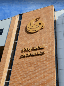
The MicroDevice Prototyping Facility (MPF) in the College of Sciences is capable of wafer scale fabrication including MEMs, opto-electronics, nano-photonics, semiconductor devices, and microfluidics. We have equipment for small scale photolithography, sputtering and electron beam deposition, lift-off, material growth, dry etching, and characterization.
| Facility | Size | Cleanroom Class | Key Tools |
|---|---|---|---|
| CREOL CNF | 2,100 sq ft | Class 100, 1000 | Raith 5200+ EBPG, PECVD, ICP etch |
| CECS Nanofab | 3,300 sq ft | Class 100, 1000 | DWL 66+, ALD, UHV PVD, Doping/oxidation Furnaces |
| MPF | 600 sq ft | Class 1000 | E-Beam Deposition |